Embedded / Tutorial
Designing an FPC NFC Tag Antenna for the nRF54L15: From KiCad to LiteVNA
A real design, fabrication and tuning case for a small NFC antenna built around the nRF54L15, from the first estimate to phone testing.
An NFC antenna is not a generic part that can be copied from a table and forgotten. It is a coil, but it is also the chip’s matching network, the PCB underneath it, the battery, the enclosure, the ferrite, manufacturing tolerances and the reader that will eventually excite it.
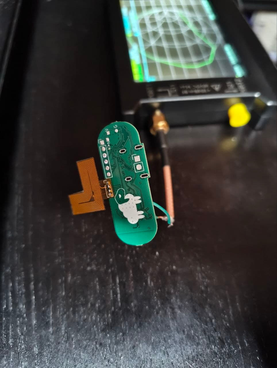
For this project we designed a very small FPC NFC tag antenna for an nRF54L15. We drew it by hand in KiCad, built several prototypes and used a LiteVNA to see what was actually happening. The calculator gave us a starting point. The lab and a phone decided what was usable.
The short version
- The antenna was designed specifically for the nRF54L15 and the space available in this product.
- We used 0.2 mm traces, 0.2 mm spacing and initially estimated 854 nH of inductance.
- The antenna measured 826 nH and 2.19 ohms without the ferrite.
- The matching capacitors were calculated using the nRF54L15 datasheet, but the actual geometry and nearby materials still required tuning.
- With the PCB and enclosure in place, the prototype reads at roughly 3 cm with a phone. That is already perfectly usable; there is still room to squeeze out a little more.
The real problem
The first step was not drawing a pretty spiral. It was deciding where the antenna could live without interfering with the rest of the hardware. The board also has a 2.4 GHz Bluetooth antenna, so the available space and the relative position of the different elements mattered from the beginning.
The NFC antenna had to fit into an awkward shape, be manufactured as an FPC and work next to a PCB, battery, enclosure and other components. A version that works beautifully while suspended in air can behave very differently once it is installed in the final product.
NFC antennas are project-specific. Even when two designs use the same standard, they cannot automatically share the same coil or capacitor values. The chip, its matching network, the antenna shape and the mechanical environment form one system.
Designing for the nRF54L15
The capacitor calculation did not come from a generic formula found at the last minute. We used the nRF54L15 datasheet, its NFC antenna configuration and the recommended matching conditions for the IC as our reference.
That gave us a sensible first value. It did not let us skip tuning. A datasheet describes the expected behaviour of the chip under reference conditions; it does not know the unusual shape of our antenna, the distance to the PCB or the ferrite sheet we would eventually add behind it.
The important point is this: the calculated capacitor is an initial hypothesis. The final antenna is designed for a specific chip and a specific integration.
From a calculator to KiCad
We chose 0.2 mm traces, 0.2 mm spacing and the number of turns needed to use the available space. An antenna calculator estimated the inductance from the geometry. Our shape was too irregular to expect perfect accuracy, so the 854 nH result was a reference, not a promise.
The schematic is deliberately boring. This type of antenna is still a coiled wire with two electrical ends: logically, it is a bridge between two connections.
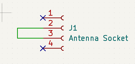
The socket has extra pads that are not part of the signal. They distribute the mechanical stress from soldering across four points instead of leaving all the strain on two connections. Copper can conduct very well, and it can also peel off with equal enthusiasm when the mechanics are neglected.
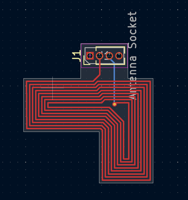
The antenna design and routing were done by hand. Automatic generators exist, but they tend to struggle with shapes this unusual and, in this case, drawing the solution took about fifteen minutes. The real time went into the calculator, the measurements and the capacitors.
What we measured before adding capacitors
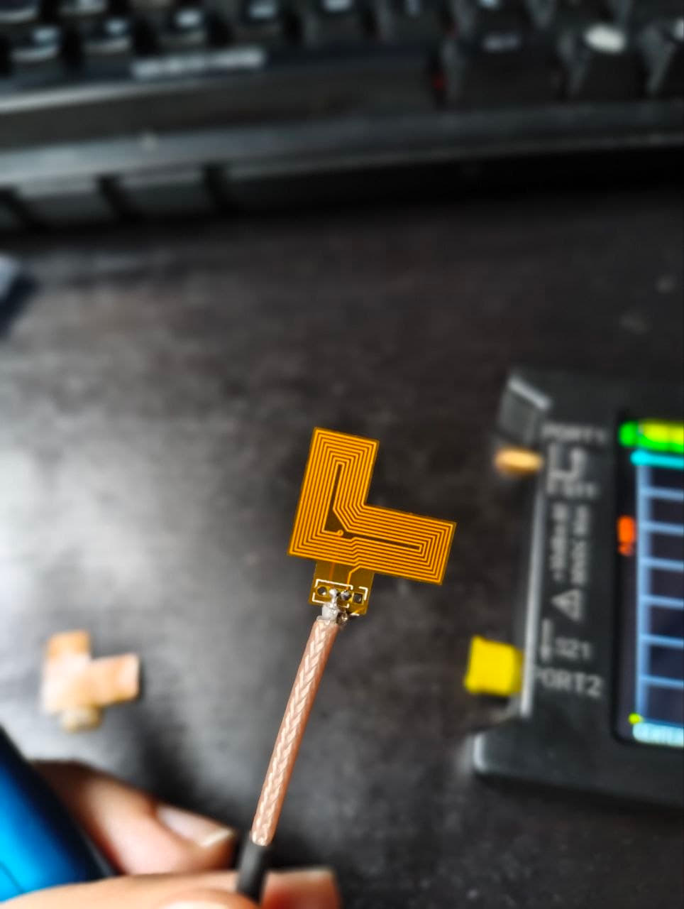
Before tuning the resonance, we measured the antenna without the matching network. The theoretical estimate was 854 nH. The practical measurement was 826 nH, much closer than expected for such an unconventional geometry.
The measured resistance was approximately 2.19 ohms. Narrow traces have a cost: the narrower the trace, the higher its resistance. The benefit is that more turns fit into the same space and increase the inductance.
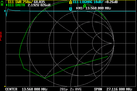
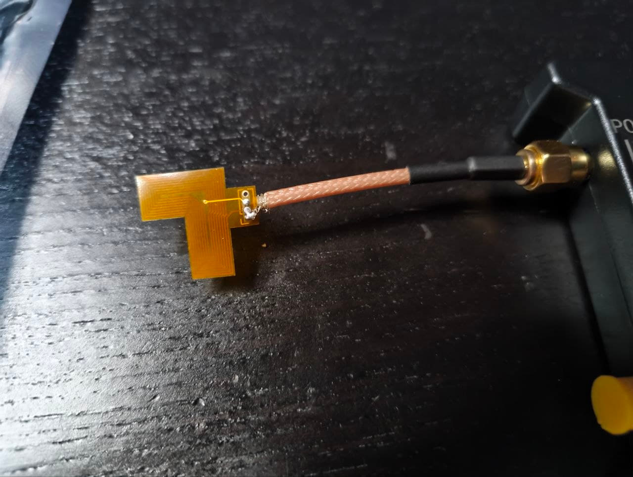
To measure an antenna this small, we used an SMA-terminated cable and connected the prototype to the LiteVNA. The connection and calibration plane matter a lot: a long cable, a poor solder joint or a badly chosen reference also become part of the measurement.
Inductance, impedance and Q
Inductance is measured in henries. Impedance is measured in ohms and describes how a circuit responds to a signal at a particular frequency. For an ideal coil, the inductive reactance can be written as:
X_L = 2π f LA capacitor provides the opposite reactance:
X_C = -1 / (2π f C)Resonance occurs when both contributions, including parasitic capacitance and losses, cancel around 13.56 MHz. In practice we are not measuring an ideal coil isolated from the universe. We are measuring the antenna, capacitors, cable, PCB and environment.
The Q factor relates stored energy to lost energy. As a simple approximation for a coil, we can think in terms of:
Q ≈ (2π f L) / RA high Q usually means lower losses and a more selective response. The goal is to get the highest Q that remains useful in the real product, not to win a Q competition with an antenna floating in the air. If Q is too high, the bandwidth becomes narrow and tolerances, enclosure, battery or tag alignment can make the system fragile.
That is why Q, inductance and impedance are parameters we can trade against each other, but always as part of the complete system. The final important measurement is whether the tag reads reliably.
Tuning the capacitors
Using the initial value calculated from the nRF54L15 datasheet and the estimated inductance, we built the first prototype with 320 pF capacitors.
320 pF: functional, but far away
The maximum resonance appeared around 9.3 MHz, far from NFC’s 13.56 MHz.
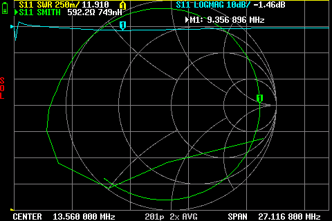
The setup worked with powerful readers, but it was not a practical solution. Something working under favourable conditions does not mean it is ready for the product.
270 pF: better, still not enough
Reducing the capacitance moved the response in the right direction. With 270 pF, the measurement at 13.56 MHz showed an impedance of approximately 6.46 ohms.
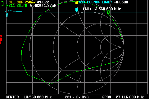
It was better than the previous prototype, but it was still not where we wanted it. With small antennas, every change looks modest until the reader starts behaving like a reviewer with very little patience.
180 pF: a much more viable result
With 180 pF, the maximum resonance moved up to approximately 15.32 MHz.
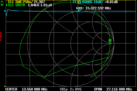
At 13.56 MHz the antenna was still inductive, and the measurement showed an impedance of approximately 139.9 ohms.
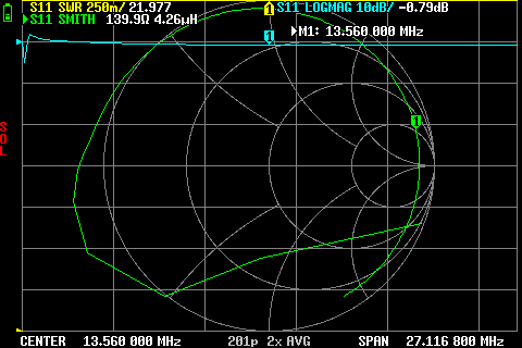
It was not a perfect paper result, but it was quite viable. In a very small tag, it can also be useful for the antenna to measure slightly above 13.56 MHz in air: once assembled with the PCB and enclosure, the resonance often shifts down.
This is not a universal rule. It is a decision based on this design, this environment and these tests.
Ferrite: the car body
We then added a 0.2 mm ferrite sheet to protect the antenna, mainly from the PCB.
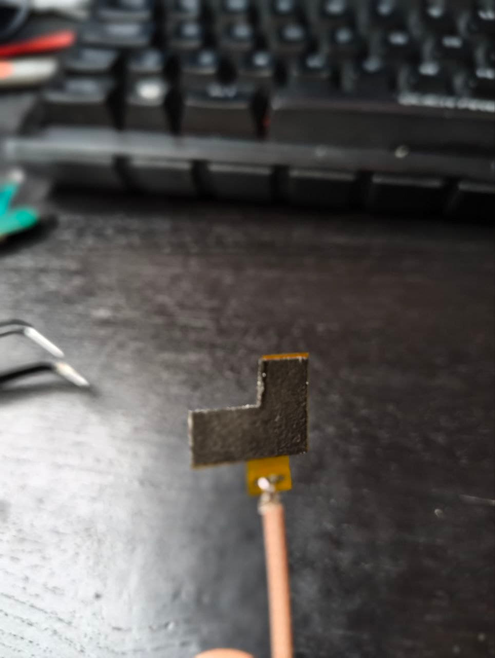
The isolated measurement got worse in one respect: resistance increased to approximately 4.4 ohms. However, inductance increased to about 1.2 uH, or 1200 nH.
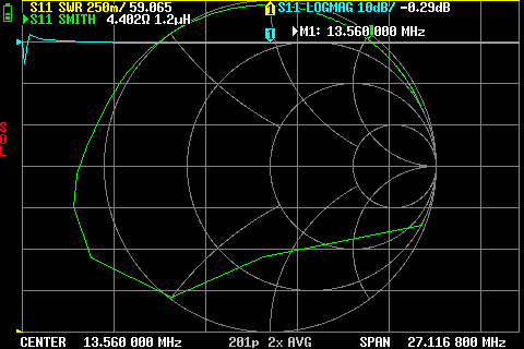
Without ferrite, the antenna looks more efficient when measured by itself. In the actual product, an unprotected antenna would be much more sensitive to the PCB and the other components. It is like saying that a car without bodywork weighs less and uses less fuel: true, but not a particularly useful configuration for driving around.
The ferrite is the bodywork. It adds losses and changes the inductance, but it lets the antenna survive its environment.
Prototypes and hand soldering
The first batch was assembled by hand with 0201 capacitors. The soldering quality is debatable, with little spikes that make the board look like an electronic hedgehog.
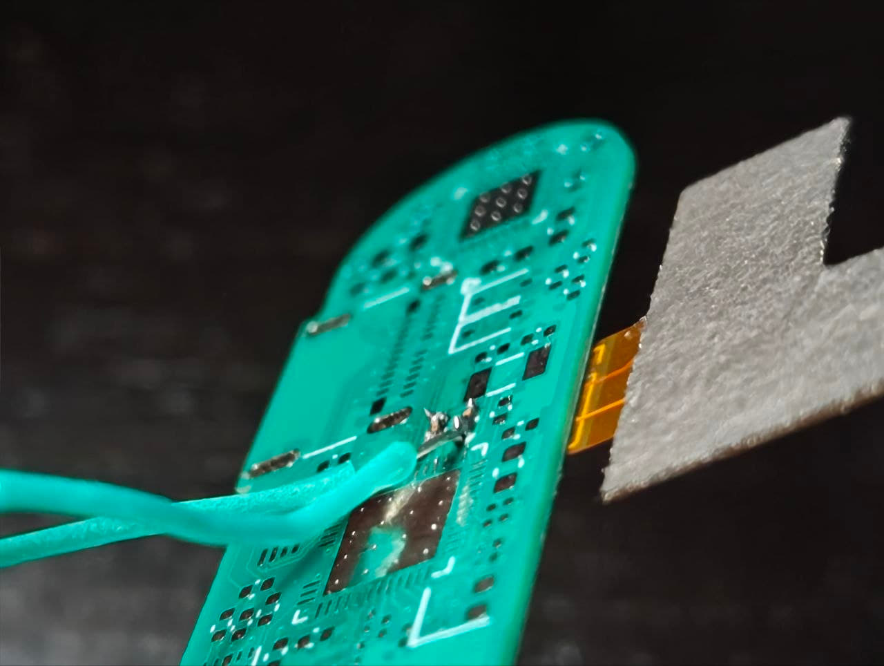
Those details can affect the measurement, but this was a lab and tinkering phase. The final prototype will use machine-placed components. Before paying for a production run, we would rather let the lab tell us which value is worth manufacturing.
With the current state, the next prototype would use 200 pF, with additional tests at 190 pF and 210 pF. That lets us observe the design’s sensitivity instead of pretending that one calculated number is magically perfect.
The test that matters: a phone
After all the calculations and all the plots, we tested the tag with a mobile phone. That is how the product will actually be used, so this test carries more authority than a pretty measurement of an isolated antenna.
With the PCB underneath and the enclosure on top, we get approximately 3 cm of reading distance with a phone. For this small tag, that is more than enough and perfectly usable in production.
We will still try to squeeze a little more out of the next prototype, but we are no longer trying to rescue a broken design. We are tuning a design that works.
Common failure modes
- Using a generic antenna without adapting it to the specific chip.
- Calculating capacitors without consulting the nRF54L15 datasheet.
- Treating a measurement in air as the final answer.
- Ignoring the PCB, battery, enclosure or ferrite.
- Confusing inductance, impedance and reactance.
- Optimising for an extremely high Q and ending up with an excessively narrow bandwidth.
- Trusting an automatic generator with a geometry that has very specific mechanical constraints.
- Declaring the antenna finished before testing it with the real reader.
Cloudy’s check
Cloudy appears on the board because even a grumpy sheep deserves an antenna that works. The rule is simple: if it only reads on the LiteVNA, it is not finished. If it reads on a phone, inside the enclosure and at a useful distance, then we can start talking.
Where this connects
This work connects hardware design, NFC, KiCad, embedded systems and product validation. It is also a good example of why antenna design does not end with a formula: it requires understanding the chip, building prototypes, measuring carefully and testing the system under the conditions in which it will actually be used.